Before starting
The objective of this project was an attempt for me to solely adventure the analog chip design process of a PLL without any help from professors or other senior colleagues. The project was executed in open source to show that anyone could do analog designs with the help of free tools that can be run on their very own personal PC.
In this series, I describe the entire design process as truly as possible — listing all the rigorous mistakes and speculations I’ve made through the process, followed by the reasons for attempting such actions. All final decisions were made solely by myself after many hours of speculation, so nothing here has been approved by anyone else; instead, I try to persuade you of each decision to the fullest.
I believe posting these mistakes will help future readers by providing realistic advice that can only be realized when tackling actual design considerations.
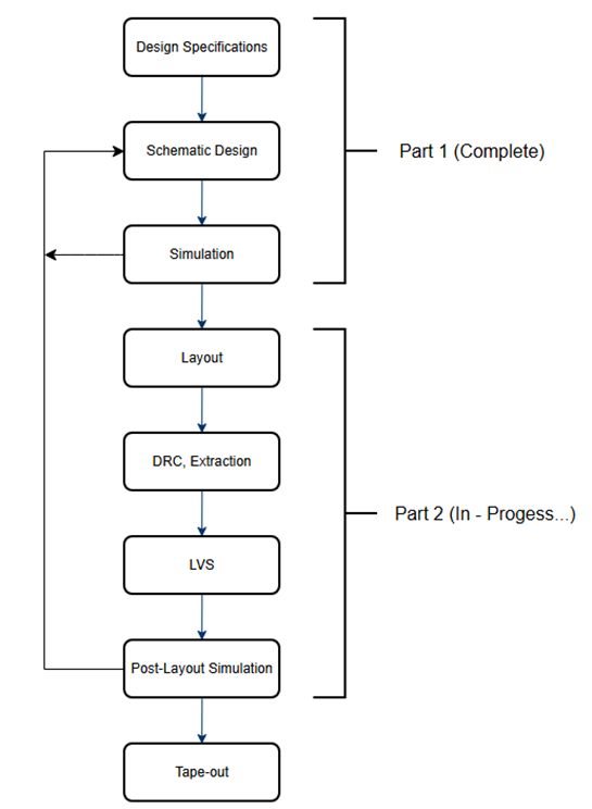
What this series covers
- Part 1 — Determining the PLL specs and simulating its schematics (complete)
- Part 2 — Layout, DRC, extraction, LVS, and post-layout simulations (in progress)
Things you need to know
This project relies on key concepts from:
- Design of Analog CMOS Integrated Circuits, 2nd Edition — Razavi [1]
- Mandatory chapters: CH15, 16 · Recommended: CH5, 7, 13
- Design of CMOS Phase-Locked Loops: From Circuit Level to Architecture Level, 1st Edition — Razavi [2]
- Mandatory chapters: CH3, 7, 8, 9, 15