Table of Contents
-
Design Simulation
2.1. Signal Analysis
2.1.1. Voltage Controlled Oscillator Signal
2.1.2. Divider Signal
2.1.3. Phase Frequency Detector Signal
2.1.4. Charge Pump Signal
-
Conclusion
3.1. Summary
3.2. Limitation
3.2.1. Noise Simulation
3.2.2. VCO Non-Linearity
3.2.3. Transistor Sizes -
Future Works
4.1. Layout
4.2. Alternative Topologies
Introduction
Now we begin the design of the Full PLL. First, we assess the PLL components into a unified topology. Next, we observe the PLL signals to analyze how the components operate in one. Afterward, we evaluate which aspects align with the theoretical approach and which do not. Finally, we discuss some of the potential future works related to this topic.
1. PLL Topology
1.1. PLL Components Assembly
Proposed PLL Topology
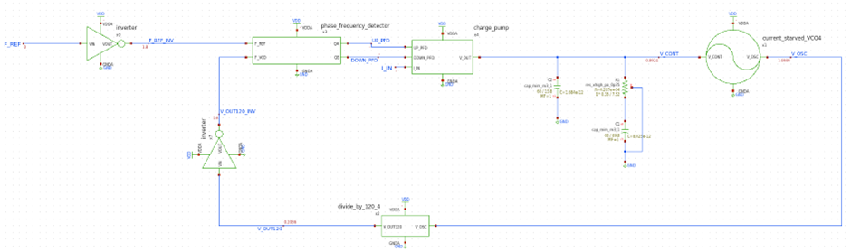
Figure 1. Proposed PLL Topology
Fig.1 is the proposed topology of the PLL components assembly. As they are named, all the components are the final designs of their post. The inverters are the only new unit in this design. This leads to faster simulations, which is possible by avoiding signals that have sharp changes such as F_REF.
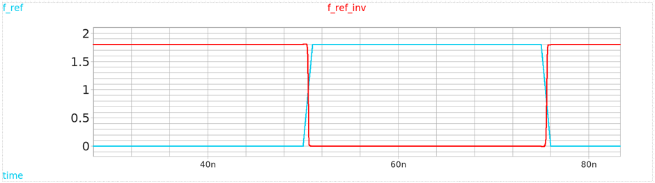
Figure 2. Inverter Output Signal
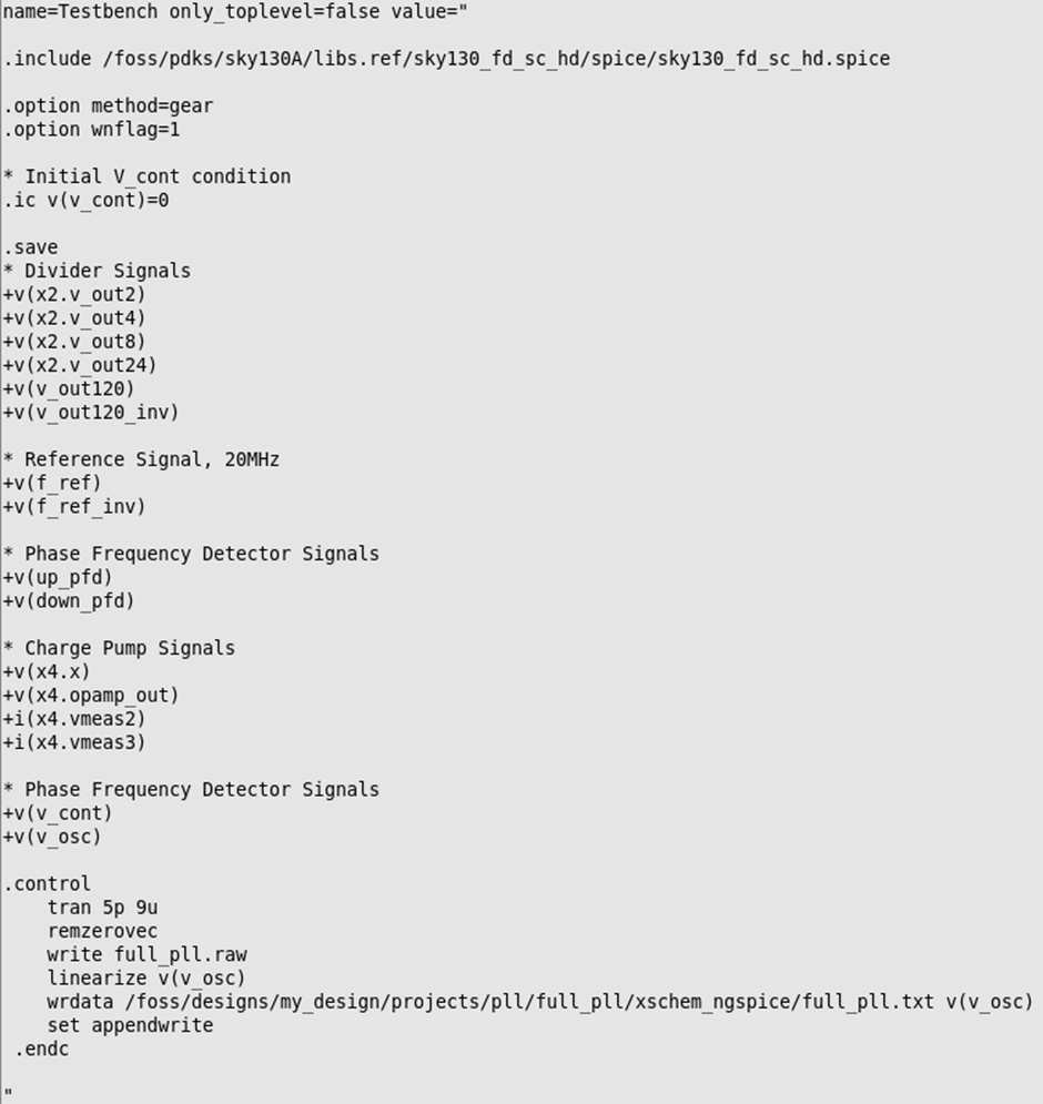
Figure 3. SPICE for the Full PLL
Fig.3 is the SPICE code for the simulations, with some description of the signals. The simulation runs for 9us to observe its stability in steady-state conditions. “V_osc” signal data were written to “.txt” files to be examined in Python. It is also important to save only the signals of interest, which will be about 300MB to our SPICE code. Avoid “save all” because it will create GBs of “.raw” data which will crash the simulation.
2. Design Simulation
2.1. Signal Analysis
2.1.1. Voltage Controlled Oscillator Signal
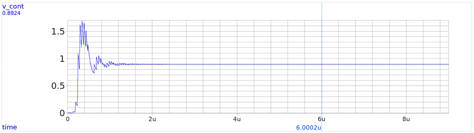
Figure 4. V_CONT for the Full PLL
Fig.4 is the simulated result of V_cont, where we can spot that the PLL successfully locks its state in a few microseconds.
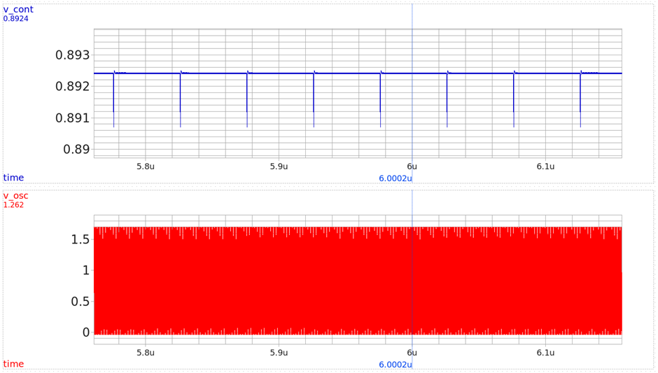
Figure 5. CLosed-up V_CONT for the Full PLL
Fig.5 is the close-up V_CONT and V_OSC signals, with y-axis scale in mV. The aspect of V_CONT is similar to the “Condition 3” in the CP design part 2 post.
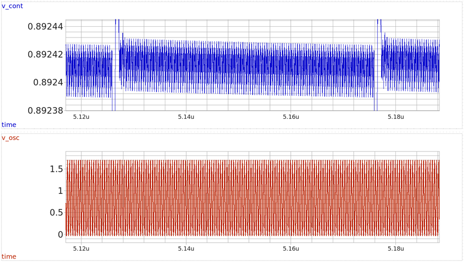
Figure 6. CLosed-up V_CONT for the Full PLL
Up close like fig.6, the actual V_CONT distorts about 0.03mVpp. This occurs from the subtle changes in the input parasitic capacitances of the VCO components when the oscillation happens. Meaning, that the distortion comes from the VCO itself and cannot be suppressed unless the MOSFETs get smaller. However, with our devices from the Skywater130PDK, which limits the MOSFET size to [W: 0.43um, L: 0.15um], this is as far as we go.
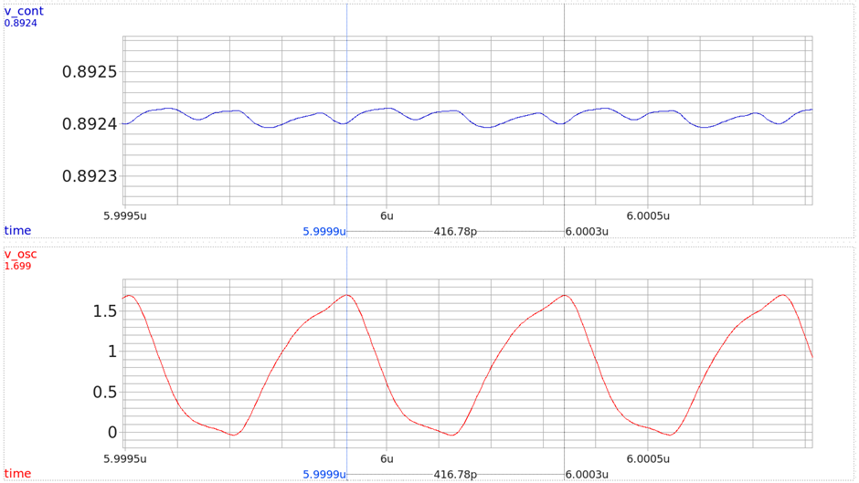
Figure 7. CLosed-up V_CONT for the Full PLL
As shown in fig.7, by scaling the x-axis to a window of approx. 1ns, we can see the actual V_OSC waveform, with the period being 416.78, precisely 2.4GHz.
2.1.2. Divider Signal
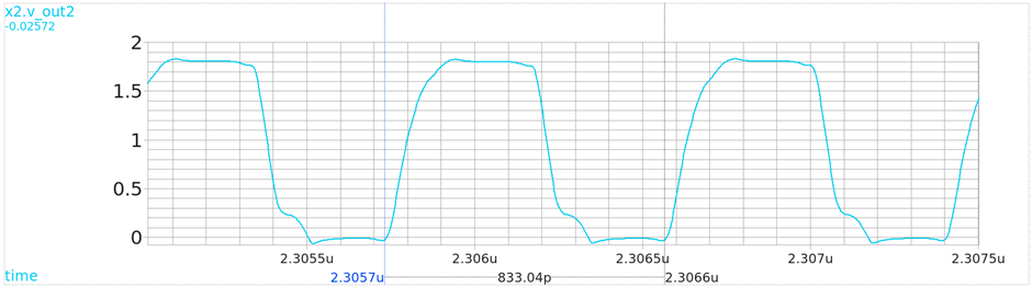
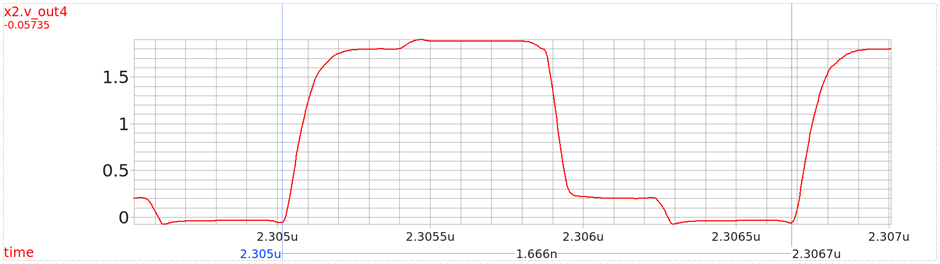
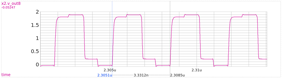
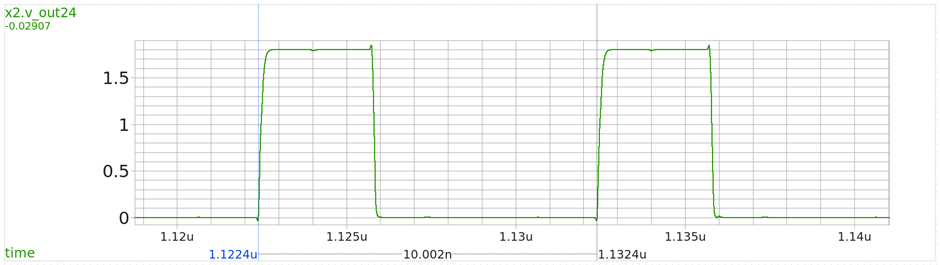
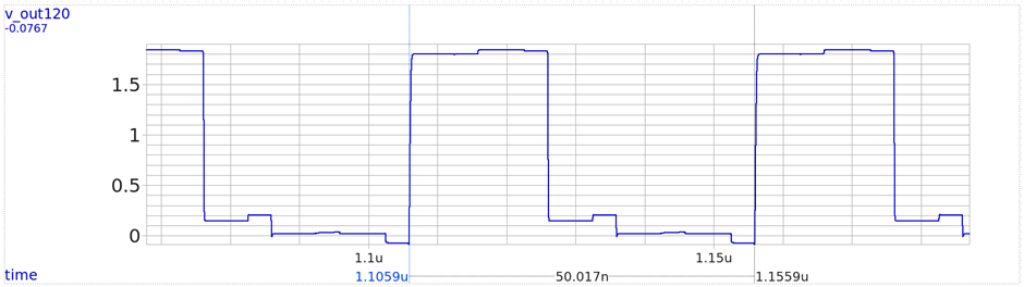
Figure 8. Divider Signals
Fig.8 is the divider signals. As the plot goes down, the period of each graph ascends respectively to the value configured in the FD section.
2.1.3. Phase Frequency Detector Signal
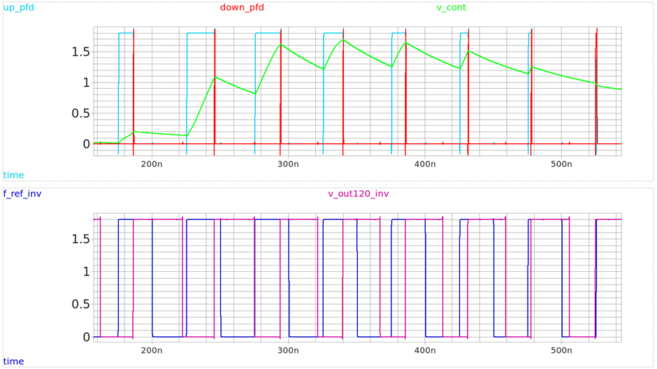
Figure 9. Phased Frequency Detector Transient State Signal
In fig.9, it shows the PFD signals in the transient state, the top plot as the PFD output signal and the bottom plot as the PFD output signal, respectively. The top plot also includes the V_cont signal to see how it reacts to the PFD measurements.
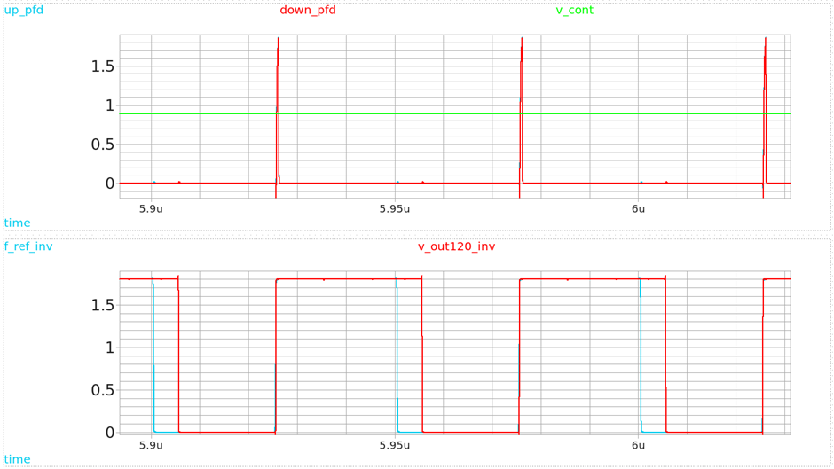
Figure 10. Phased Frequency Detector Steady State Signal
In fig.10, shows the PFD signals in the steady state, meaning they are in the lock-state of V_cont as approx. 0.887V.
The bottom plot is the PFD input signals and notice how the signal from the divider does not meet the duty cycle of 50%. Yet, our PFD is a positive edge-detecting component, leading to the outputs in the top plot. It releases the least pulse it can create, which is the minimum state transition time of the logic gates.
2.1.4. Charge Pump Signal
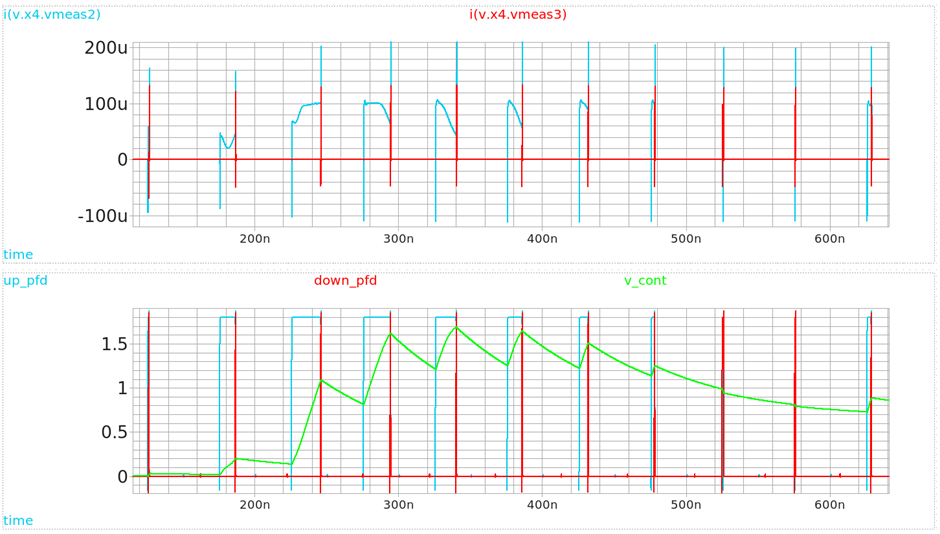
Figure 11. Charge Pump Transient State Signal
In fig.11, shows the CP currents in the transient state, it tries to provide currents up to 100uA.
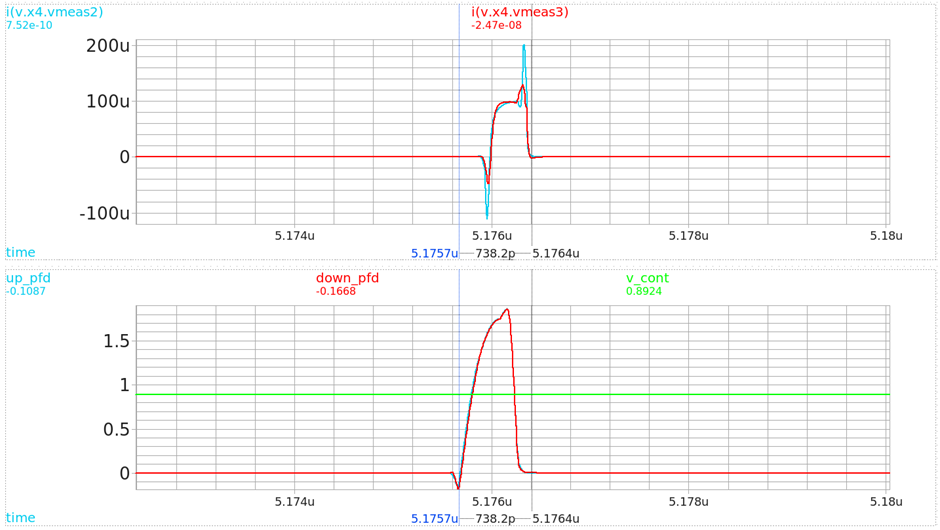
Figure 12. Charge Pump Steady State Signal
In fig.12, shows the CP currents in steady state, providing 100uA.
3. Conclusion
3.1. Summary
From the observation of signal analysis, we achieved the top priority. Designing a PLL that outputs a 2.4GHz signal by locking at a certain V_cont. The MOSFET size of the CP has been significantly decreased, and the FD has been developed in TSPC topology. This led to a dramatic reduction in the overall size of the topology.
3.2. Limitation
3.2.1. Noise Simulation
Ngspice, the simulation tool for this project, has limitations in noise simulations. Referring to the online forums of this OSIC tool, it lacks the ability to produce and execute transient noise simulation in high frequencies. Sadly, this matter cannot be addressed, unless such features are enhanced, or we use a different tool.
3.2.2. VCO Non-Linearity
From fig.11, it is ambiguous that the CP is providing exactly 100uA. The first reason is the insufficient current from the reference current branch in initial conditions. This is the trait of using an OPAMP to create a replica circuit for current mirroring. Second, using a modest OPAMP could have caused the mismatch. Its design is too simple and has limitations for being not fully rail-to-rail leading to imperfections.
3.2.3. Transistor Sizes
Currently, the skywater130pdk provides MOSFETs down to [W: 0.43um, L: 0.15um] in the smallest dimensions. This restricts the capabilities in some components such as the VCO, where the parasitic capacitances cause small distortions to V_cont, as well as the operating frequencies of the overall topology.
4. Future Works
4.1. Layout
After completing the schematic simulations to meet our objectives, we can now move on to implementing this design in MAGIC VLSI where we could draw the layout for this circuit. DRC, LVS, and PEX would be our next steps in the design process. This work is expected to be done soon.
4.2. Alternative Topologies
Many challenges yet await in this PLL. They could be listed as,
- VCO in an LC oscillator
- Improved OPAMP for this CP
- Alternative CP topology
- Alternative PFD topology
- Alternative loop filter designs
- Digital Locked Loops
Among these, the practical ones might be the topic of the LC oscillator to practice the implementation of inductors in MAGIC VLSI and Skywater130pdk. The second plan would be the Digital Locked Loops, where the main focus would be to exercise digital circuit design to prepare for mixed circuit designs.
Next post, the full topology of the PLL will be put under analysis.
Discussion
Comments
Share questions, corrections, or notes through GitHub.