Target Architecture
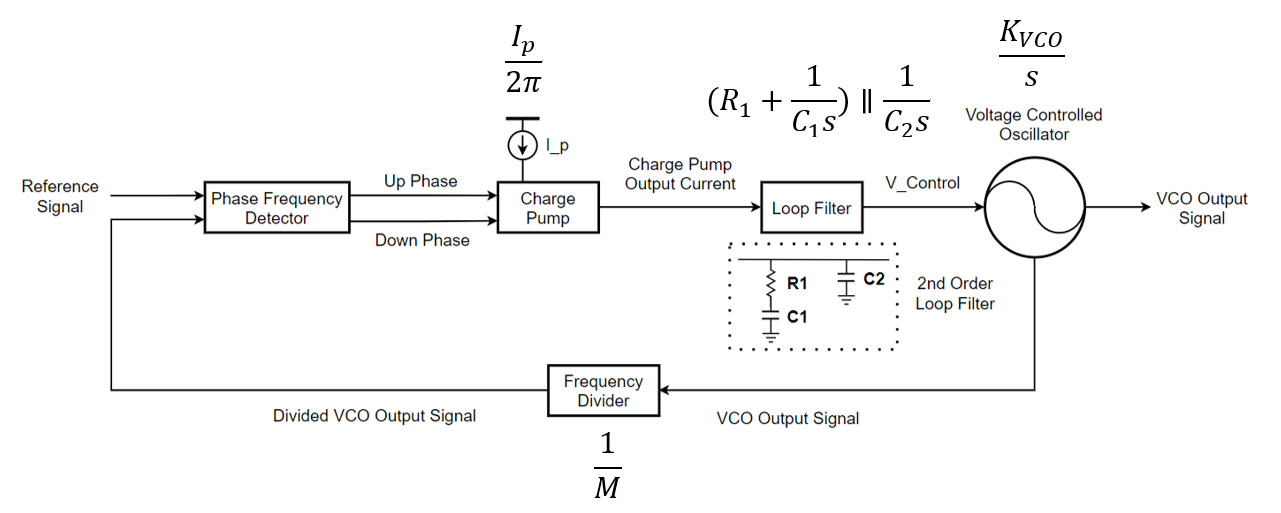
Our target architecture will look like this. One thing to point out is that it is a 3rd order PLL with a 2nd order loop filter.
Configuring Design Parameters
However, when we are determining the design parameters, we define a 2nd order PLL with a 1st order loop filter.
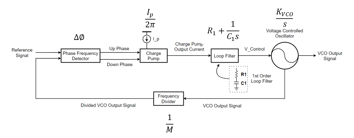
This is because, if the PLL is set as 2nd order, we can use control theory to analyze the 2nd transfer function. This enables the analysis of natural frequency and damping factor, while a 3rd order transfer function can’t be easily analyzed through such simple methods.
Consideration for C2 in the Loop Filter
After analysis, we place into the loop filter, surmising it will have a small effect on the system.
As a rule of thumb, is normally set to 0.1~0.2 of the value of .
Transfer Function
We start with this equation, which is the transfer function of the PLL, assuming is linear for now:
Simplified:
Design Parameters
The design parameters are as follows:
- : Charge pump reference current [A]
- : Voltage-to-frequency gain of the oscillator [Hz/V]
- : 1st order loop filter capacitor [F]
- : 1st order loop filter resistor [ohms]
- : Divider ratio (dimensionless)
Trade-Offs in Analog Circuit Design
In analog circuits, everything comes with a trade-off. Enhancing Feature A might degrade Feature B, and decisions should be made based on design priorities. After deriving and loop filter values, we’ll explore how changing these values affects the system.
Initial Design Procedure
-
F_VCO : The VCO output frequency is 2.4 GHz.
-
F_REF : For phase detection, was set to 20 MHz.
- This results in , which can be factored as .
- This allows for experimentation with divide-by-2, divide-by-3, and divide-by-5 blocks.
-
I_p : Arbitrarily set to 100uA as a starting point.
Why use arbitrary values for I_p?
The value of the charge pump does not effect the its topology.
Rather, the actual CONVICT is the operation of charge pumps. In particular, its switching stages are what matters in the topology decision, which we will discuss later in the charge pump design section.
C1, R1, and K_vco?
These three cannot be decided unless we get our hands on the Kvco values.
Kvco is “the ratio of output frequency with respect to input voltage” of a given topology.
Meaning we need to find out the frequency of the VCO output signal at a given voltage, and this needs to be measured after the schematic simulation of VCOs, it’s not something we can guess right off the bat
To conclude, this post covers the initial considerations for our PLL design. In the next post, we’ll dive into the VCO implementation.
Discussion
Comments
Share questions, corrections, or notes through GitHub.